Engineering
Feb 19, 2026
Engineering
Inside NVIDIA DGX Spark: Is DGX Spark Actually Blackwell?

Jeongkyu Shin
Founder / Researcher / CEO

Kyujin Cho
AI Platform Architect
Feb 19, 2026
Engineering
Inside NVIDIA DGX Spark: Is DGX Spark Actually Blackwell?
Jeongkyu Shin
Founder / Researcher / CEO
Kyujin Cho
AI Platform Architect
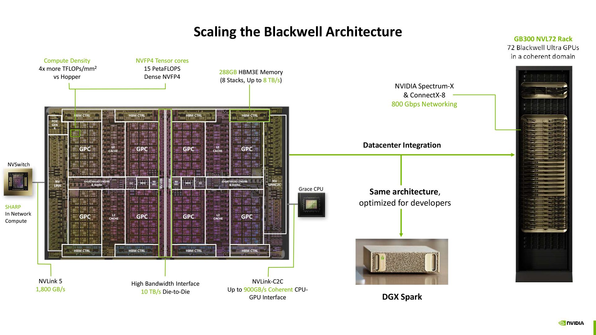
Scaling the Blackwell Architecture, © NVIDIA
In October 2025, NVIDIA released the DGX Spark, a compact AI supercomputer designed to bring datacenter-class AI performance to a desktop form factor. Built on the Grace Blackwell architecture, the DGX Spark packs 128GB of unified memory and 1 PFLOP of AI compute into a 150mm x 150mm chassis, enough to run and fine-tune large language models up to 200B parameters locally. At Lablup, we bought 20 units shortly after launch and have been running them in-house since.
GLM-5 and Sparse Attention
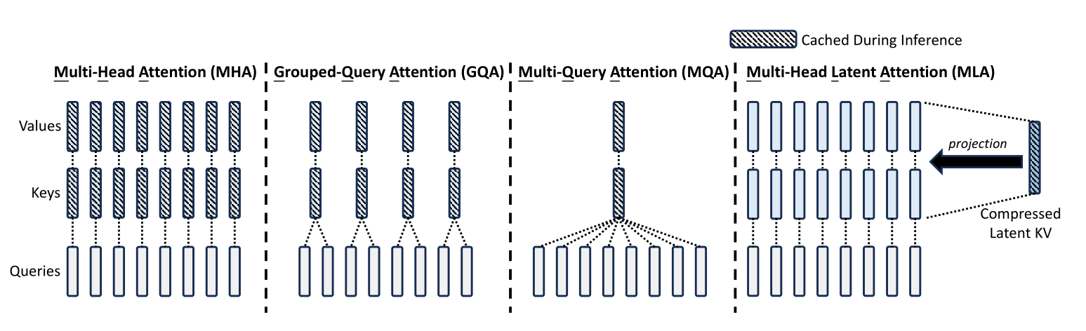
Different KV caching techniques, © [liorsinai.github.io](https://liorsinai.github.io/machine-learning/2025/02/22/mla.html)
Our engineering team recently tried running GLM-5 inference on DGX Spark. GLM-5 uses two techniques together: MLA (Multi-head Latent Attention) and DSA (DeepSeek Sparse Attention). When a large language model generates text, it stores Key and Value vectors from previously processed tokens in a memory region called the KV cache,1 and this cache grows rapidly as models get bigger and inputs get longer. MLA compresses the cache into lower-dimensional vectors to save memory, while DSA reduces compute by dynamically selecting only the important tokens for attention calculation instead of attending to every token. MLA was first introduced in DeepSeek-V2 and later adopted by DeepSeek-V3 and GLM-5. GLM-5 adds DSA on top of that, improving both long-context performance and deployment cost. Running these techniques efficiently on GPUs requires specialized kernels,2 and the two most prominent implementations today are DeepSeek's FlashMLA and FlashInfer.
Both projects explicitly list Blackwell support, so we expected them to work on DGX Spark. They did not. FlashMLA ships two backends: one for SM100 (datacenter Blackwell) and one for SM90 (Hopper). The DGX Spark GPU reports as SM12x (compute capability 12.1), which is compatible with neither. The SM100 kernel requires the tcgen05 instruction and TMEM, a dedicated hardware memory for tensor operations. The SM90 kernel requires WGMMA. SM12x has none of these. FlashAttention had the same problem: SM12x is absent from the supported architecture list, and the runtime printed "FlashAttention only supports Ampere GPUs or newer." FlashAttention 4 (FA4), the Blackwell-specific version under development, only supports SM100.
DGX Spark is Blackwell. The kernels claim to support Blackwell. So why don't they work? Answering that question required looking more carefully at what's inside GB10.
Inside GB10
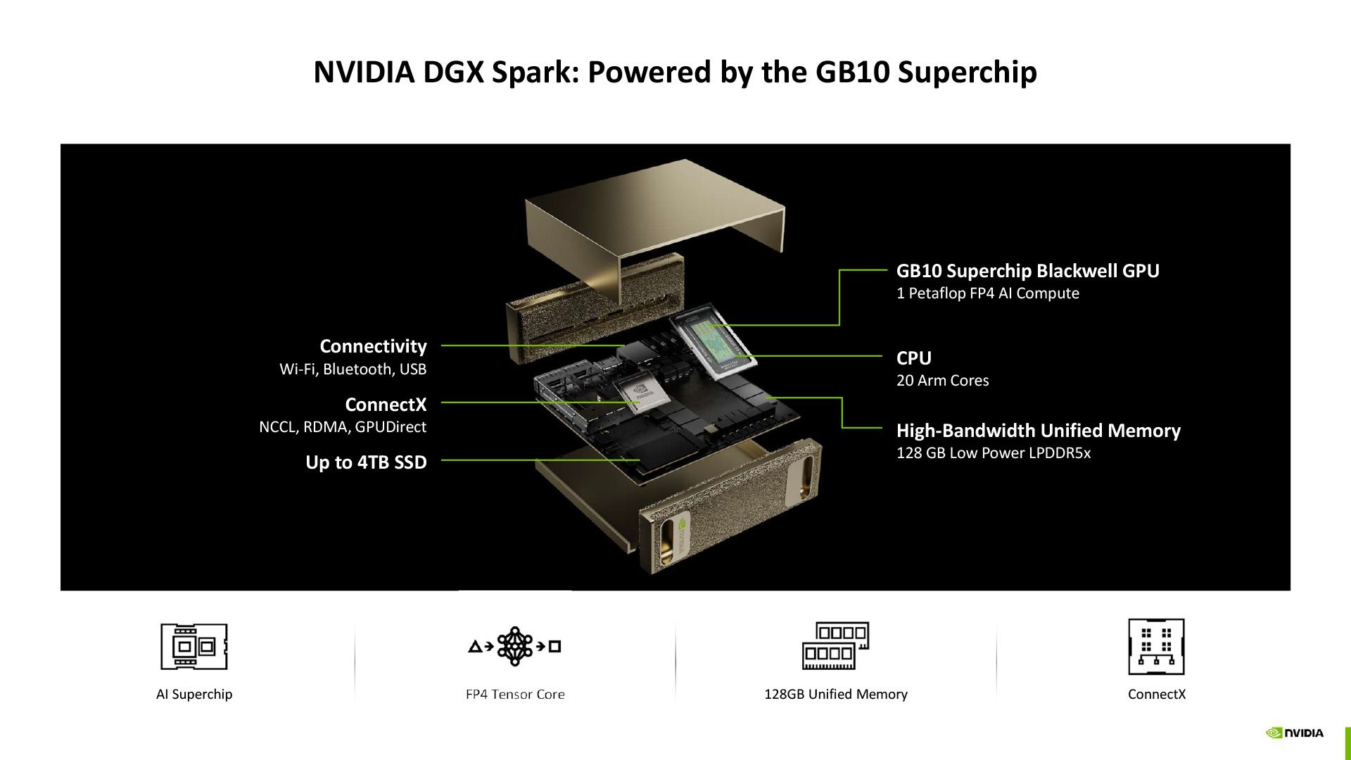
NVIDIA DGX Spark: Powered by the GB10 Superchip, © NVIDIA
GB10 is a multi-die SoC co-designed by NVIDIA and MediaTek. A TSMC 3nm ARM CPU die (ten Cortex-X925 cores plus ten Cortex-A725 cores) connects to a Blackwell GPU die via NVLink C2C, and 128GB of LPDDR5X memory is shared between the CPU and GPU at 273 GB/s bandwidth. The GPU side has 48 SMs,3 6,144 CUDA cores, and delivers 1 PFLOP at sparse FP4. In terms of raw scale, it sits between the RTX 5070 and RTX 5070 Ti. Run nvidia-smi and the architecture field reads 'Blackwell.' NVIDIA calls GB10 a "Grace Blackwell Superchip." There is no reason not to call it Blackwell.
But check the compute capability,4 and a different picture starts to emerge.
Two Blackwells: SM100 and SM12x
CUDA's compute capability numbering reveals that Blackwell is not a single architecture. Datacenter and consumer/edge parts carry different compute capabilities.
| Datacenter Blackwell | Consumer/Edge Blackwell | |
|---|---|---|
| Compute Capability | 10.0 (SM100) | 12.0 (SM120) / 12.1 (SM121) |
| Products | B100, B200, GB200 | RTX 5090 (SM120), DGX Spark (SM121) |
| Shared memory per SM | 228 KB | 128 KB |
| Max concurrent warps5 per SM | 64 | 48 |
| TMEM (tensor memory) | 256 KB per SM | None |
| Tensor core instruction | tcgen05 (5th gen dedicated) | Extended mma.sync (Ampere-style) |
| Warpgroup MMA | WGMMA supported | Not supported |
| Multicast/cluster | 2+ SMs can cooperate | Each SM executes independently |
RTX 5090 is SM120, DGX Spark is SM121. I'll refer to both as SM12x throughout this post.
The compute capability numbers split into 10.x and 12.x, and this is not like the Ampere situation where 8.0 and 8.6 diverged within the same major version. The major numbers themselves are different, and 11.x is entirely vacant. Looking back across Pascal (6.0/6.1), Ampere (8.0/8.6), and Hopper/Ada (9.0/8.9), no generation has produced this wide a gap. CUTLASS build flags reflect the split too: datacenter targets use sm100a (architecture-accelerated) while consumer targets use sm120f (family-level), with different suffix conventions.
Tensor Core Instruction Differences
Tensor cores are the dedicated hardware that GPUs use to accelerate matrix multiplication, the core operation of deep learning. The instruction set (ISA6) that drives these tensor cores has changed with each generation.
| Generation | Instruction | Who issues it | Reads data from | Writes result to |
|---|---|---|---|---|
| Volta through Ampere (SM 7.x/8.x) | mma.sync | Warp (32 threads) | Registers | Registers |
| Hopper (SM 9.0) | wgmma | Warpgroup (128 threads) | Shared memory | Registers |
| DC Blackwell (SM 10.0) | tcgen05.mma | Single thread | Shared memory | TMEM (dedicated hardware memory) |
| Consumer Blackwell (SM 12.x) | Extended mma.sync | Warp (32 threads) | Registers | Registers |
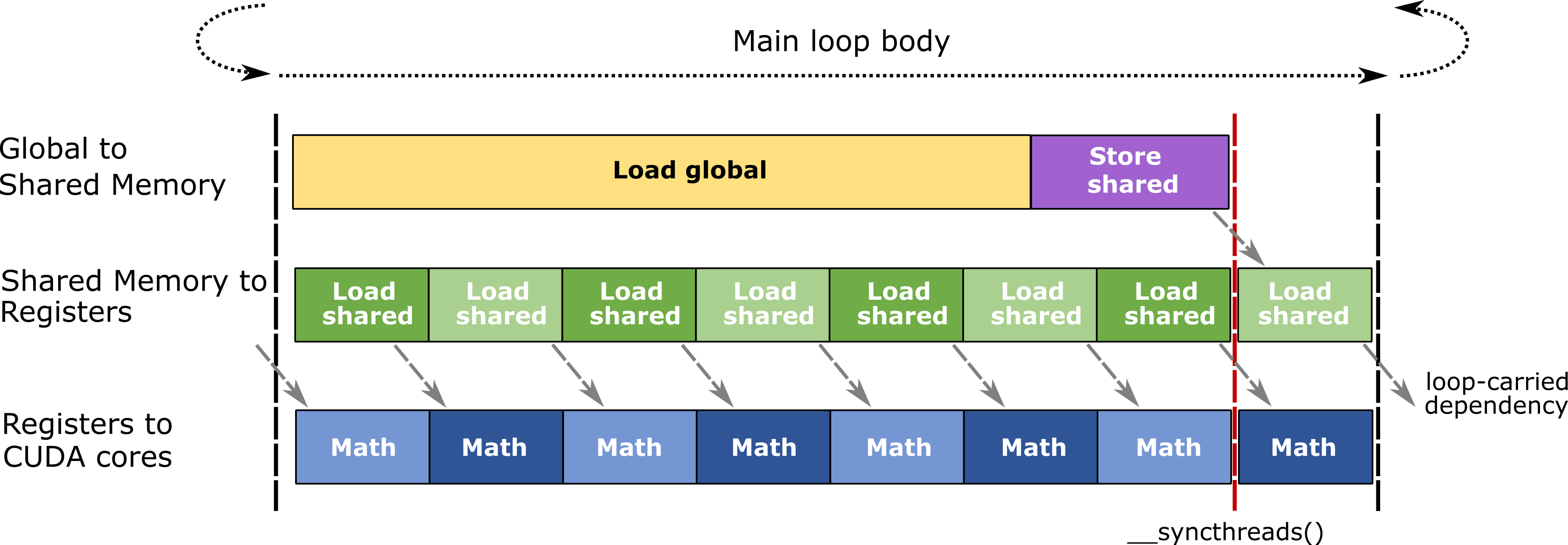
Eficient, pipelined mainloop body used in CUTLASS GEMMs, © [NVIDIA](https://github.com/NVIDIA/cutlass/blob/2.11/media/docs/efficient_gemm.md)
Matrix multiplication works by chopping large matrices into small tiles and computing them iteratively. Each tile's intermediate result (the accumulator) needs to be stored somewhere temporarily. From Volta through Hopper, these intermediate results lived in the register file,7 where CUDA cores and tensor cores had to share the same limited space. Datacenter Blackwell (SM100) added TMEM, a dedicated 256KB-per-SM hardware memory sitting next to the tensor cores, along with the tcgen05 instruction to control it. Tensor cores can now operate independently from CUDA cores without competing for register file bandwidth. That is the single biggest architectural change in SM100.
SM12x lacks the TMEM hardware entirely, and therefore does not support the tcgen05 instruction that controls it. The same goes for Hopper's WGMMA: compiling WGMMA code targeting SM12x produces ptxas error: Instruction 'wgmma.fence' not supported on .target 'sm_120'. The tensor core instruction that SM12x actually uses is an extended version of mma.sync, the same instruction family that dates back to Ampere. It adds support for new numeric formats like FP4 and FP6, but the programming model itself is the oldest one available. Looking at the last column of the table, SM100 writes intermediate results to dedicated memory (TMEM), while SM12x reads from and writes to registers, exactly like Ampere. Datacenter Blackwell turned the tensor core into an autonomous compute unit; consumer Blackwell put new data types on top of the oldest programming model.
Because SM90 kernels use WGMMA, SM100 kernels use tcgen05, and SM12x kernels use extended mma.sync, there is no kernel compatibility among the three architectures. Developers have to maintain three separate code paths.
Porting existing kernels to SM12x is not straightforward, either. A 64x64 matrix tile that SM100 processes in one operation must be broken into 16x8 chunks requiring 32 separate mma.sync calls. Memory load patterns, inter-thread synchronization, and thread organization all need to be redesigned.
Finding the patterns from the past
NVIDIA shipping different microarchitectures under the same generation name is not new to Blackwell. In the Ampere generation (2020), the datacenter GA100 (A100) was manufactured on TSMC 7nm with 64 FP32 cores per SM and HBM2 memory. The consumer GA102 (RTX 3090), released the same September, used Samsung 8nm, had 128 FP32 cores per SM, and shipped with GDDR6X. GA102 repurposed the Turing-era INT32 datapath to also handle FP32 operations, doubling the shader count per SM, while GA100 skipped that change to focus on FP64 compute and HBM bandwidth. Different fabs, different SM designs, different memory interfaces, same "Ampere" branding.
With Hopper/Ada Lovelace (2022), NVIDIA separated the names outright. Datacenter Hopper (H100, SM90) was announced in March 2022; consumer Ada Lovelace (RTX 4090, SM89) followed in September as a distinct architecture. Compute capabilities were different too: 9.0 for Hopper, 8.9 for Ada Lovelace.
In Pascal (2016), GP100 (Tesla P100) had NVLink and HBM2; GP102 (GTX 1080 Ti) had neither.
The Design Logic
Datacenter chips and consumer chips allocate their transistor budgets differently. Datacenter parts spend die area on FP64 compute, HBM memory bandwidth, NVLink/NVSwitch, and MIG partitioning. Consumer parts spend on RT cores, display outputs, and power efficiency. The entire GB10 SoC runs at 140W; a single B200 GPU draws 1,000W.
SM100's TMEM, tcgen05, and 2-SM cooperative MMA are designed for datacenter environments where thousands of GPUs process massive matrix operations. Models like GLM-5 and DeepSeek-V3 use MoE8 architectures that activate only a subset of the model's parameters (expert subnets) per input token, so instead of running one large matrix multiply for a long time, they rapidly switch between many smaller ones. TMEM absorbs the accumulator storage pressure during these switches, and tcgen05's asynchronous execution allows prefetching the next expert's weights while the current expert is still computing. On a DGX Spark, where LPDDR5X provides 273 GB/s of memory bandwidth, the bottleneck is getting data from memory to the compute units, not tensor core throughput. Investing die area in TMEM and tcgen05 would yield little practical benefit under those conditions. SM12x keeping the proven mma.sync approach while adding FP4/FP6 support, 5th-gen tensor cores, and RT cores reflects this tradeoff. At Hot Chips 2025, NVIDIA disclosed that GB10 worked on TSMC 3nm A0 (first silicon) without revision, because it was assembled from validated IP blocks rather than designed from scratch.
Where the Software Ecosystem Stands
FlashMLA's sparse decoding kernel internally uses FP8 KV cache together with either WGMMA- or tcgen05-based matrix multiply. Neither is available on SM12x, so an SM12x backend would need to be written from the ground up. FlashInfer is in the same situation. FlashAttention's supported architecture list includes only Ampere, Ada Lovelace, and Hopper, and the runtime does not recognize SM12x as "newer than Ampere." FlashAttention 4 (FA4) supports SM100 only. In the vLLM and SGLang ecosystems, SM12x-related issues keep surfacing. The most common: FP8 block-scaled GEMM kernels written for SM100 fail to run on RTX 5090 (SM120). SGLang's published DeepSeek-V3 serving configurations include H200 (SM90) and B200 (SM100) setups, but nothing for SM12x.
Triton treats SM12x as SM80 (Ampere), disabling all Blackwell-related optimizations, and vLLM requires the --enforce-eager flag. Running attention kernels on SM12x is not entirely impossible: some developers have reported re-implementing FlashAttention in CUDA C++ using Ampere-era instructions (mma.sync, cp.async) or falling back to cuDNN's SDPA backend. These workarounds only support standard dense attention, though. MLA-specific kernels, sparse attention, and FP8 KV cache are out of reach, which makes it difficult to get full performance from models like GLM-5 or DeepSeek-V3.
One thing DGX Spark does offer that conventional desktops cannot: its 128GB of memory is shared between CPU and GPU without partitioning. A discrete GPU setup physically cannot do this. The bandwidth is lower than HBM, but being able to fit an entire 200B-parameter model in memory on a desktop machine is a rare capability. Once SM12x-native kernels materialize, the practical value of that memory pool changes considerably.
Looking Forward
GB10 is Blackwell. It has 5th-gen tensor cores, supports FP4/FP6 arithmetic, and includes RT cores. What it does not share with datacenter Blackwell is the instruction set. SM12x's tensor core programming model is closer to Ampere's mma.sync than to datacenter Blackwell's tcgen05, and for kernel developers, that means maintaining three separate code paths: Hopper, datacenter Blackwell, and consumer Blackwell.
This kind of datacenter-versus-consumer architectural split has recurred in every generation since Pascal, and the gap is wider in Blackwell because datacenter-only features like TMEM and tcgen05 are larger in scope than anything that came before. While a $4,000 desktop device cannot possibly contain the full instruction set of a $30,000+ data center GPU, the existence of instruction-level branching under the same 'Blackwell' name is an engineering detail worth noting for developers writing or relying on CUDA kernels.
Try Backend.AI GO on DGX Spark. Supports DGX Spark's Unified Memory natively, for free.
Footnotes
-
KV cache: A memory region where language models store Key and Value vectors from previously processed tokens. As models grow larger and inputs grow longer, this cache scales proportionally. ↩
-
Kernel: A program that runs on the GPU. Here, it refers to attention computation code that has been hand-optimized for specific GPU hardware. ↩
-
SM (Streaming Multiprocessor): The basic compute building block of an NVIDIA GPU. Each SM contains CUDA cores and tensor cores, and overall GPU performance is determined by how many SMs a chip has and how each is configured. ↩
-
Compute Capability: A version number NVIDIA assigns to indicate a GPU's hardware feature level. GPUs within the same generation receive different numbers if they support different instructions and features. ↩
-
Warp: A group of 32 GPU threads that move in lockstep, executing the same instruction simultaneously. The fundamental unit of execution in GPU programming. ↩
-
ISA (Instruction Set Architecture): The set of instructions that hardware understands. Just as CPUs have x86 or ARM, GPUs have their own instruction sets, and two chips branded 'Blackwell' with different ISAs cannot run the same compiled code. ↩
-
Register file: The fastest storage available, sitting right next to the processor core. Its limited capacity means contention arises when multiple operations try to use it simultaneously. ↩
-
MoE (Mixture of Experts): A model architecture that activates only a subset of 'expert' subnetworks per input, rather than using the entire model every time. This reduces actual compute relative to total parameter count. ↩