Nov 6, 2026
Releases
MLxcel 0.8 "Eyes Wide Open" – Eyes on AMD Strix Halo

Lablup
Lablup

Jeongkyu Shin
Founder / Researcher / CEO
Nov 6, 2026
Releases
MLxcel 0.8 "Eyes Wide Open" – Eyes on AMD Strix Halo
Lablup
Lablup
Jeongkyu Shin
Founder / Researcher / CEO
MLxcel 0.8, the LLM/VLM inference engine developed by Lablup, is out. With 590 commits since 0.7.0, the biggest change in this release is broader hardware support. Alongside Apple Silicon and NVIDIA CUDA, MLxcel now has a ROCm backend for AMD GPUs, and Windows 11 gains native inference through both CUDA and ROCm.
There is a lot more in 0.8. Starting with this version, most model families run native batched decode under the --parallel option, and a bundled WebUI with a model library and chat screen launches with a single --webui flag. We also added nine image generation models, including FLUX.2 Klein and Qwen-Image-2.1, along with vision models such as SAM 3 and DINOv2. Cluster communication for distributed inference now uses per-connection authentication and encryption.
This post focuses on one part of the release: MLxcel's support for AMD Strix Halo. Based on the session we presented at AMD Advancing AI World Tour & AI DevDay Seoul 2026 on November 4, we cover what Strix Halo is, why its unified memory architecture matters now, and what we ran into while porting the ROCm backend, along with the results.
TL;DR
To use MLxcel on Strix Halo, build from source on Linux with ROCm installed and the rocm feature enabled.
As of v0.8.1, we do not yet ship prebuilt binaries for ROCm.
git clone https://github.com/lablup/mlxcel.git
cd mlxcel
cargo build --release --features rocm

# Interactive run (the model is downloaded automatically on first run)
./target/release/mlxcel run mlx-community/Qwen3-30B-A3B-4bit

# OpenAI-compatible server + WebUI, 4 concurrent requests
./target/release/mlxcel-server -m mlx-community/Qwen3-30B-A3B-4bit --port 8080 --parallel 4 --webui
Here is a summary of what we measured on a Ryzen AI MAX+ 395 (Radeon 8060S, gfx1151):
- All 44 models we tested ran successfully, covering dense, MoE, and VLM models in 4-bit, FP8, and MXFP4 formats.
- Nemotron 3 Nano 30B-A3B, with 3B active parameters, decodes at 75.9 tok/s.
- Gemma 4 31B, a dense 31B model, decodes at 10.2 tok/s, close to the theoretical ceiling set by memory bandwidth (about 10.8 tok/s). Its prefill runs at 315 tok/s, faster than llama.cpp on Vulkan (260 tok/s).
- The ROCm backend is still experimental and has only been validated on gfx1151, the GPU in Strix Halo.
What is Strix Halo?
Strix Halo is the development codename for AMD's Ryzen AI Max 300 series, announced in early 2025. Strix is Latin for owl and also the scientific name of a genus of owls. AMD uses the name for its Zen 5–based mobile chip family, and the mainstream laptop chips in that family are called Strix Point. Halo, in industry terms, refers to the top-of-the-line product that represents a brand. Strix Halo, in other words, is the flagship of the Strix family. That is also where the name of the 0.8 release, Eyes Wide Open, comes from: like a wide-eyed owl, MLxcel is widening its view of supported hardware beyond Apple Silicon.
What sets Strix Halo apart from conventional laptop chips is that it puts a large GPU and a wide memory bus into a single package. Key specs for the top model, the Ryzen AI Max+ 395:
| Component | Specification |
|---|---|
| CPU | Zen 5, 16 cores / 32 threads, up to 5.1GHz |
| GPU | Radeon 8060S, RDNA 3.5, 40 CUs, up to 2.9GHz (gfx1151) |
| NPU | XDNA 2, up to 50 TOPS (126 TOPS platform total) |
| Memory | 256-bit LPDDR5X-8000, up to 128GB, 256 GB/s theoretical bandwidth |
| GPU-allocatable memory | Up to 96GB |
| Power | 45–120W (cTDP) |
* Sources: AMD product page, Tom's Hardware
Strix Halo also includes an NPU separate from the GPU, in order to meet Microsoft's Copilot+ PC specification. Copilot+ PC certification requires an NPU of at least 40 TOPS, at least 16GB of memory, and at least 256GB of storage, and meeting those requirements unlocks Windows' on-device AI features. Strix Halo's 50 TOPS NPU clears that bar.
That said, an NPU in the 40–50 TOPS class is designed to run lightweight, always-on AI features at low power. It is not enough to run LLMs with billions of parameters. So the NPU handles Windows' AI features, while large-model inference falls to the 40-CU GPU and the large pool of unified memory. MLxcel uses the GPU.
Other vendors are taking a similar approach. At Computex 2026, NVIDIA unveiled its Windows PC chip, previously known as N1X, under the name RTX Spark. It combines a 20-core Arm Grace CPU and a Blackwell RTX GPU in a single package, and Dell, HP, ASUS, Lenovo, MSI, and others are shipping systems with it starting this fall (Tom's Hardware, The Federal). Jensen Huang has said that the GB10 used in DGX Spark is a variant of the N1 line (Winaero). The CPU architecture differs, x86 versus Arm, but the recipe is the same: a big GPU, wide unified memory, and an NPU. The AI PC market is moving toward unified memory.
What is unified memory?
A unified memory architecture (UMA) is one in which the CPU and GPU share the same physical memory. In a typical PC, the CPU has its own system memory (DRAM), a discrete GPU has its own dedicated memory (VRAM), and data moving between the two is copied over the PCIe bus. With unified memory, that copy goes away, because the CPU and GPU read and write tensors at the same addresses.
A brief history
Unified memory is not a new idea. Various companies have been developing it in their own ways for more than a decade, and it is getting renewed attention as demand for running AI models locally grows.
| Year | Platform | Significance |
|---|---|---|
| 2013–2014 | AMD Kaveri APU, hUMA | First hardware implementation of HSA, in which the CPU and GPU share a virtual address space and read each other's memory without copying data |
| 2014– | NVIDIA Jetson family | CPU and GPU share a single LPDDR memory on an embedded SoC |
| 2020 | Apple M1 | Brought to mainstream desktops and laptops a design in which the CPU, GPU, and Neural Engine share a single on-package memory pool |
| 2023 | NVIDIA GH200 | Combines the Grace CPU's LPDDR5X (up to 480GB) and the Hopper GPU's HBM3 (96GB) over 900 GB/s NVLink-C2C into a single coherent address space |
| 2025 | NVIDIA GB10 (DGX Spark) | CPU die and GPU die share 128GB of LPDDR5X as one physical and logical memory |
| 2025 | AMD Strix Halo | Unified memory APU for x86 laptops and mini PCs, with up to 96GB available to the GPU |
Sources: Electronic Design, Apple announcement, Chips and Cheese, ServeTheHome
When AMD announced hUMA in 2013, the goal was to cut the time GPUs spent waiting for data. Back then, the main beneficiaries were graphics and general-purpose GPU compute. More than a decade later, the same architecture is back in the spotlight because of LLMs.
Why unified memory matters for AI
LLM inference, and especially the decode phase that generates tokens one at a time, is shaped more by memory bandwidth than by compute. Every token requires reading the model weights from memory once. Unified memory helps in two ways.
The first is capacity. Consumer discrete GPUs typically have 24–32GB of VRAM, which leaves little headroom even for a 30B-class model quantized to 4 bits. On Strix Halo, where the GPU can use 96GB, 30B-class models and even larger ones fit entirely in memory.
The second is that it suits MoE (Mixture-of-Experts) models. Many recent open models use an MoE design: the total parameter count is large, but only a subset of experts is activated for each token. On a discrete GPU, if the whole model does not fit in VRAM, the overflow expert weights have to be pulled across the PCIe bus. Since which experts get selected depends on the data, compute can stall on every token while expert weights are transferred. The staging copy, which places the weights on the host side once more, can also double memory use and bandwidth consumption. With unified memory, the entire sparse checkpoint sits in memory, and each token reads only the weights of the experts it activates. Decode speed then depends only on memory bandwidth.
There is a catch. Strix Halo's theoretical bandwidth of 256 GB/s is more than an order of magnitude lower than the HBM on datacenter GPUs (GH200's HBM3 runs at 4 TB/s). On unified memory devices, then, an MoE model with few active parameters runs much faster than a dense model of the same total size. We will see this difference in numbers in the benchmarks below.
Unified memory, done differently
Even among unified memory designs, where the memory controller sits varies by vendor. On GB10 it is on the CPU die, on Strix Halo it is on the I/O die that also holds the GPU, and on Apple Silicon it is on the SoC die that holds both CPU and GPU.
| Platform | Memory controller location | CPU–GPU link | Memory pool | Bandwidth |
|---|---|---|---|---|
| Apple Silicon | Same SoC die as the CPU, GPU, and Neural Engine | Direct, on the same die | One coherent pool | 68 GB/s on M1, higher on larger chips |
| NVIDIA GB10 | CPU die (S-die), designed by MediaTek | NVLink C2C, 600 GB/s bidirectional | Single 128GB pool | 301 GB/s (LPDDR5X-9400) |
| AMD Strix Halo | Large I/O die (IOD), shared with the GPU and NPU | Two Zen 5 CCDs attached to the IOD via die-to-die links | Two pools split at boot (on our test system: 96GiB GPU, ~31GiB OS) | 256 GB/s (LPDDR5X-8000) |
On GB10, the memory controller is on the CPU die, so the GPU reaches memory through the C2C link. NVIDIA has said it did performance modeling with MediaTek to make sure GPU memory traffic gets enough bandwidth even when it passes through MediaTek's memory subsystem. Strix Halo is the opposite. The GPU, the memory controllers, and a 32MB MALL cache all sit on the same IOD, with the CPU chiplets attached alongside. In other words, memory sits closest to the GPU. The trade-off is that the CPU cores cannot use the GPU's last-level cache.
The difference that matters most for an inference engine is how the memory pool is divided. On Apple Silicon and GB10, the operating system and the GPU share one pool. Strix Halo sets aside a GPU carve-out in firmware ahead of time, so the memory the OS sees is not the same as the memory the GPU can use. The problems this caused during porting are covered in the next section.
More flexibility on Linux with GTT
On Linux, there is another option besides a BIOS carve-out: allocating GPU memory dynamically through the GTT (Graphics Translation Table). According to AMD's documentation, the Strix Halo GPU accesses system memory through GPU virtual memory (GPUVM), so memory is not physically divided but simply mapped. GTT allocations are not permanently reserved, which means the operating system can reclaim that memory while the GPU isn't using it.
The default GTT limit is about 50% of system memory, or a little over 60GB on a 128GB machine. AMD recommends keeping the dedicated VRAM in the BIOS small, around 0.5GB, and raising the kernel's TTM page limit (/sys/module/ttm/parameters/pages_limit) instead. The older amdgpu.gttsize parameter is increasingly being replaced by TTM settings. When the GTT limit is larger than VRAM, the driver also serves VRAM allocation requests from GTT.
# Check and change the current limit with AMD's debug tools (reboot required)
pipx install amd-debug-tools
amd-ttm              # Show the current TTM limit
amd-ttm --set 100    # Allow the GPU to use up to 100GB of shared memory

# Or set it directly as a kernel parameter (in 4KiB pages; this example is 120GiB)
ttm.pages_limit=31457280
Here is how the two approaches compare:
| Item | BIOS carve-out | GTT |
|---|---|---|
| How memory is reserved | Fixed at boot; the OS can't use it even when the GPU is idle | Allocated on demand; the OS reclaims it when the GPU isn't using it |
| Maximum GPU memory | Up to 96GB | Up to the kernel limit Many users set it to around 120GB on 128GB machines |
| Changing the setting | Enter the BIOS | Kernel parameter or amd-ttm; reboot required |
| GPU memory as seen by the engine | Reported directly as device memory | Only a small VRAM region may be visible, so the GTT size has to be read separately |
| Contention with the OS | Fixed boundary; neither side encroaches on the other | Both share one pool, so setting the limit too high can starve the OS of memory |
| Support | Independent of the OS | Linux only; requires a kernel with the KFD fixes for Strix Halo |
The biggest advantage of GTT is that memory never sits idle. If you carve out a fixed 96GB, the OS can't touch that memory even when no model is loaded. With GTT, the GPU takes memory only when it needs it, and the limit can be set higher than 96GB, putting large MoE models approaching 100GB within reach.
There are some caveats, though.
- Engines read memory size differently. In a GTT setup, the VRAM reported by HIP can come out small. The Strix Halo fork of vLLM was changed to read the GTT size directly from sysfs (randomvariable/vllm), and there is a proposal in llama.cpp to adjust memory detection on Strix Halo systems that use TTM allocation (llama.cpp #18159). Which value an engine uses for its memory budget matters far more here than with a carve-out.
- Leave room for the OS. Because the OS and the GPU share one pool, setting the limit too close to total memory can leave the OS out of memory the moment a large model loads. The community typically leaves a few GB for the OS.
- Measure performance yourself. Some report no difference between preallocated VRAM and GTT, while others report VRAM being faster. There are also reports that disabling the IOMMU raises memory bandwidth by 5–10%, but these have not been verified yet (Framework community).
All measurements in this post were taken with a 96GiB BIOS carve-out, so that they could be compared with the native Windows ROCm build we developed alongside it.
Porting ROCm to Strix Halo
Test environment
All measurements in this post were taken on a Ryzen AI MAX+ 395 (Radeon 8060S, gfx1151) system running Debian 13 with ROCm 10.0 (HIP 7.15). The firmware carves out 96GiB for the GPU, leaving roughly 31GiB for the operating system.
RDNA 3.5 and wave32
The Radeon 8060S is an RDNA 3.5 GPU. The feature that helped most during porting was wave32. AMD GPUs call the group of threads that executes an instruction together a wavefront, and RDNA runs 32 threads per wavefront by default. That is the same width as a CUDA warp or a Metal simdgroup, so kernel logic written around warp-level reductions and shuffles carried over without major changes.
There are differences, too. Matrix operations go through WMMA (Wave Matrix Multiply-Accumulate) instructions, which support 16x16x16 bf16 and f16 operations. Probing with hipBLASLt showed support for bf16 and int8 but not fp8, and there are no FP4 matrix instructions at all. Here is how the three platforms compare:
| Item | ROCm (RDNA 3.5, gfx1151) | Metal (Apple Silicon) | CUDA (NVIDIA) |
|---|---|---|---|
| SIMD width | wave32 (wave64 on CDNA) | simdgroup 32 | warp 32 |
| Matrix ops | WMMA 16x16x16, bf16/f16 | simdgroup matrix | Tensor Cores |
| FP8 / FP4 compute | None; decoded in software | None; decoded in software | FP8 from Hopper, FP4 on Blackwell |
| Memory | Unified, split into two pools | Unified, single pool | Discrete VRAM across PCIe |
| Kernel build | Mostly AOT, some hipRTC JIT | Generated at runtime, then cached | NVRTC JIT, then cached |
| After a GPU fault | Every HIP call fails until the process exits | Error reported via MLX events | Sticky error until reset |
The Metal and CUDA columns describe general platform characteristics; they were not measured on the Strix Halo system.
One numerical quirk is worth knowing about. On gfx11-series GPUs, WMMA in bf16 and f16 returns −2⁻²⁴ rather than 0 for 1 + (−1). The error is within the bounds of a standard f32 dot product, but it needs to be accounted for when writing tests that compare results bit for bit.
How RDNA and CDNA differ
AMD GPUs come in two architectural lines: RDNA, used in Radeon cards and APUs, and CDNA, used in Instinct datacenter accelerators. Both are programmed with ROCm and HIP, but the hardware is quite different.
| Item | RDNA (Radeon, Strix Halo) | CDNA (Instinct MI300X, MI355X, etc.) |
|---|---|---|
| Default wave width | wave32 (wave64 mode available) | wave64 |
| Matrix ops | WMMA instructions (from RDNA 3) | Dedicated Matrix Cores and MFMA instructions |
| Low-precision formats | No FP8 or FP4 matrix instructions on gfx1151 | Hardware support up to FP8 and FP4, depending on generation |
| Memory | LPDDR, GDDR | HBM |
Even if the same HIP source compiles for both, a kernel tuned for wave32 and WMMA will not perform the same on wave64 and MFMA. MLxcel's ROCm backend has so far only been validated on gfx1151, so results on other hardware may differ.
At its main Advancing AI 2026 event this summer, AMD said that CDNA 5 (MI455) has been redesigned on an RDNA foundation, effectively dropping wave64 in favor of wave32 execution (Chips and Cheese). As the two architectures converge again, the wave32 kernels we wrote for Strix Halo can serve as a starting point when we add CDNA support.
mlxcelverse: how we extend hardware support
First, a quick look at MLxcel's architecture. The CLI and the OpenAI-compatible server are the entry points. The control plane, which covers model loading and auto-detection, tokenizers, multimodal pipelines, and the batch scheduler, is written in Rust. The data plane, which handles the generation loop, KV cache, sampling, and speculative decoding, is a C++ core that calls into the hardware execution layer through an FFI bridge. On Apple Silicon, MLX's Metal runtime provides that execution layer; on other hardware, mlxcelverse does.
mlxcelverse is a project that collects overlays on top of MLX along with custom kernels specific to MLxcel. The CUDA, ROCm, and OpenXLA backends all live there, and each overlay records the MLX commit it is based on. Our ROCm backend started from NripeshN/mlx (MIT license), a community ROCm fork of MLX. It was proposed upstream as an experimental ROCm backend in June 2025 (ml-explore/mlx #2300) and consists of 106 new backend files and about 43,900 lines of code.
Rather than applying the fork as patches, we brought it in as file-level overlays. The ROCm overlay in mlxcelverse consists of 111 backend files and 16 MLX core files, and at build time those files are copied wholesale on top of the MLX commit MLxcel pins. It is the same pin that the Metal and CUDA builds use, and the ROCm files are applied only in ROCm builds.
- Bumping the pin never causes patch conflicts. Because files are replaced whole, there is no patch fuzz and no risk of the same hunk being applied twice.
- Every pin bump is checked for drift. The offline check runs as part of
make verifyand finishes in two seconds; if you bump the MLX pin on a Mac without updating the ROCm overlay, it fails immediately.
Porting timeline
| Date (2026) | Milestone |
|---|---|
| Sep 11 | Spike: fork builds standalone, all 42 op tests pass |
| Sep 12 | Overlay merged into mlxcel |
| Sep 30 | First throughput baseline on gfx1151 |
| Oct 15 | ROCm epic closed, 12,384 tests passing |
| Oct 21 | v0.8.0-beta.1 released |
| Oct 26 | Native Windows build, native NVFP4 kernels |
| Nov 1–2 | v0.8.0 and v0.8.1 released |
It took about five weeks from the spike to closing the ROCm epic. Along the way, we fixed 70 defects in the fork, most of which also exist in the community fork.
| Category | Problem | Fix |
|---|---|---|
| Grid limits | 32-bit grid arithmetic prevented launching kernels with 2³² or more threads, and one kernel never wrote its last 257 elements | Switched to 64-bit grid-stride loops |
| Thread safety | No locks on BLAS handles, the JIT cache, or the event pool; an 8-thread test failed 20 out of 20 runs | Added locks; 0 failures in 20 runs |
| Quantization kernels | Wrong scale strides and dtype branches produced NaNs or relative errors up to 1e34 for MXFP4 and MXFP8 | Fixed strides and branches |
| Missing ops | FFT, Hadamard, and SearchSorted were empty stubs that called std::terminate | Implemented as native HIP kernels |
| GPU fault handling | After a queue fault every HIP call fails, but wait functions blocked forever | Wait functions now return an error |
| Build system | Editing a header did not rebuild HIP objects (0 of 41) | Header changes tracked via dependency files |
Alongside the fixes, we put validation in place. A self-hosted gfx1151 runner checks the ROCm build, linking, and actual generation in CI, and the same checks can be run locally with make verify-rocm.
Unified memory pitfalls
We mentioned earlier that Strix Halo splits its memory into two pools. In practice, that split caused more trial and error than anything else.
- Budget memory against the device pool. Before loading a model, MLxcel calculates whether it will fit in memory. If that calculation is based on the OS's free memory, it sees only about 31GiB, and even the 26GB Mixtral gets skipped. We now budget against the 96GiB device pool. Builds and CPU reference runs, on the other hand, have to fit within the roughly 31GiB of OS memory.
- The GPU waits during CPU fallback. We initially handled NVFP4 dequantization on the CPU, and the GPU sat idle for about one second of a 1.5-second prefill. The cause was that the CPU reads the GPU's share of memory uncached. That work now runs on the GPU.
- Shared cache lines produce wrong results without errors. In a multi-threaded OpenBLAS environment, reading tightly packed GPU scalars could pick up stale cache lines, silently returning wrong results. We fixed this by limiting BLAS to one thread and widening the spacing between scalar slots to 128 bytes.
- Cap the amount of in-flight GPU work. The host was submitting work every 2,000 operations without waiting for the GPU to finish. Once we capped in-flight work, peak memory for Llama 3.1 8B 4-bit dropped 3.4×, from 20.6GB to 6.1GB, with no change in decode speed.
How this differs from the OpenXLA + IREE path
MLxcel already had one path for hardware beyond Apple Silicon: the OpenXLA backend, available in alpha since v0.6.0. It exports models as StableHLO graphs and has the IREE compiler generate code for the target hardware, targeting accelerators such as TPUs and NPUs. IREE itself supports AMD GPUs through HIP (see the IREE documentation), so in theory this path could have covered Strix Halo as well.
We still chose a native ROCm backend because the two paths are fundamentally different.
| Item | Native ROCm (mlxcelverse) | OpenXLA + IREE |
|---|---|---|
| Approach | Runs MLX ops directly on the AMD GPU | Hands the model graph to a compiler for code generation |
| Model support | Uses the same model code as Metal and CUDA | Graph path must be ported per model family |
| Input shapes | Dynamic lengths, continuous batching, paged attention | Requests assigned to the smallest precompiled context size that fits |
| Optimization | Hand-written fused HIP kernels | Compiler optimizations |
| Maturity | Experimental, validated on gfx1151 | Alpha |
The native path means writing kernels by hand for each backend, but in return, all 167 architectures MLxcel supports and its full set of serving features work on Strix Halo as is. We plan to keep developing the compiler path as a way to support accelerators that have no MLX backend.
Results
44 models, all working
Our first bar for the port was compatibility. From the 167 architectures mlxcel supports, we picked 44 models and measured each one once on v0.8.1 with ROCm 10.0, using a 512-token prefill and 128-token decode (pp512/tg128) at batch 1. We re-ran the 8 models whose results came out unusually low. The set covered dense, MoE, and VLM models in 4-bit, FP8, and MXFP4, and all 44 ran successfully. The figures below are absolute throughput rather than ratios against mlx-lm, because the Python MLX reference implementation does not run on ROCm.
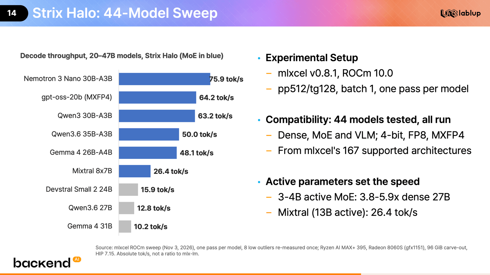
Decode speed tracks the number of active parameters, not total parameters. MoE models with 3–4B active parameters run at 48–76 tok/s, fast enough for interactive use and 3.8–5.9× faster than a dense 27B model. Mixtral 8x7B, with 13B active parameters, lands in between at 26.4 tok/s. The MoE advantage of unified memory described earlier shows up clearly in the numbers.
Decoding block floating-point formats in software
gfx1151 has no FP8 or FP4 matrix instructions. So for low-precision formats that share a scale per block, such as MXFP4, MXFP8, and NVFP4, weights are converted to fp16 or bf16 inside the kernel and then multiplied with FMA or WMMA. In the implementation we started from, this was the slowest path, and it is also where we saw the biggest gains.
| Item | Model, conditions | Before | After | Speedup |
|---|---|---|---|---|
| MXFP4 prefill | gpt-oss-20b, 512 tokens | 7.5 tok/s | 526 tok/s | 70× |
| MXFP4 decode | gpt-oss-20b | 8.3 tok/s | 63.6 tok/s | 7.6× |
| NVFP4 prefill | Nemotron-Cascade-2 30B-A3B, 512 tokens | 329 tok/s | 1,008 tok/s | 3.1× |
MXFP4 prefill got 70× faster after we switched to a kernel that processes work grouped by expert. On the decode side, the old per-row kernel had been taking about 100ms of each 115ms step. NVFP4 prefill got 3.1× faster once we moved dequantization to the GPU and used WMMA. Two implementation techniques worth mentioning:
- Branchless bit placement. FP4 (E2M1) is a 4-bit value with 1 sign bit, 2 exponent bits, and 1 mantissa bit. We write each 4-bit value directly into the sign, exponent, and mantissa bit positions of an fp16 without any conditional branches, then correct the 2⁻¹⁴ exponent offset with a single multiply at the end. This is an exact decode, not an approximation.
- Choosing WMMA based on row count. On RDNA 3.5, the fused WMMA kernel was faster than dequantizing and then calling hipBLASLt only when there were fewer than 128 rows to process. So we pick the path based on measured row count, and the NVFP4 WMMA tile kicks in from 16 rows per expert.
Profiling set the porting order
The community fork implemented MLX's basic ops, but not the fused kernels MLxcel uses on Metal and CUDA. Our initial plan was to port to HIP the kernels with the most calls first. Once we measured actual GPU execution time, though, the priorities looked different: the SSM update came out on top, while fused add-RMSNorm and RoPE fell further down the list.
| Ported kernel | Model, conditions | Decode speedup |
|---|---|---|
| Paged attention | Llama 3.1 8B 4-bit, 32K context | 1.77× |
| SSM update | Granite 4.0-H Tiny | 1.46× |
| SSM update | Nemotron-3-Nano | 1.45× |
| Paged attention | Llama 3.1 8B 4-bit, 16K context | 1.40× |
| Sampler | Llama 3.1 8B | 1.11× |
| Fused MoE | Qwen3-30B-A3B | 1.02× |
Speedups compare batch-1 decode tok/s before and after each kernel was ported. Paged attention was measured on the server path.
Profiling showed that dense and hybrid models bottleneck in different ways. For dense models like Llama 3.1 8B, decode time was concentrated almost entirely in a single kernel: qmv_wide accounted for 95% of GPU time, reading memory at about 192 GB/s. For hybrid models that mix in Mamba-style layers, the bottleneck was the sheer number of kernel launches. Generating one token took 2,000–3,200 kernel launches, leaving a gap of about 5ms on the host side per token. That is why we ported the SSM update kernel first.
The memory wall: Gemma 4 31B across engines
To see how much of the hardware MLxcel can use on a dense model, we compared it with other engines on Gemma 4 31B, a dense 31B 4-bit model.
| Engine | Backend | Prefill | Decode |
|---|---|---|---|
| mlxcel v0.8.1 | ROCm | 315 tok/s | 10.2 tok/s |
| llama.cpp | ROCm | No public figure | 10.5 tok/s |
| llama.cpp | Vulkan | 260 tok/s | 10.9 tok/s |
| llama.cpp (QAT model) | Vulkan | 276 tok/s 5,471-token prompt, server run | 10.3 tok/s |
All rows use 4-bit weights, and the measurements come from different machines. The llama.cpp figures are taken from llama.cpp GitHub Discussion #23659 (May 2026), a Gemma 4 31B benchmark report on the EVO-X2 (June 2026), and strix-halo-guide (July 2026).
Decode lands between 10.2 and 10.9 tok/s in all four cases, a spread of less than 7%. That is because the ceiling on decode speed is set by memory bandwidth, not by the engine. Dividing the 212 GB/s bandwidth measured in the EVO-X2 report by the 19.6GB weight size gives about 10.8 tok/s. Since every token requires reading all of the weights once, no engine can exceed that figure. MLxcel's decode speed is already close to that ceiling.
Prefill, by contrast, is bound by compute, so differences between engines show up. In prefill, MLxcel reaches 315 tok/s, ahead of llama.cpp on Vulkan at 260 tok/s.
Bandwidth utilization by model
Estimating bandwidth utilization per model the same way makes the gap between dense and MoE models even clearer.
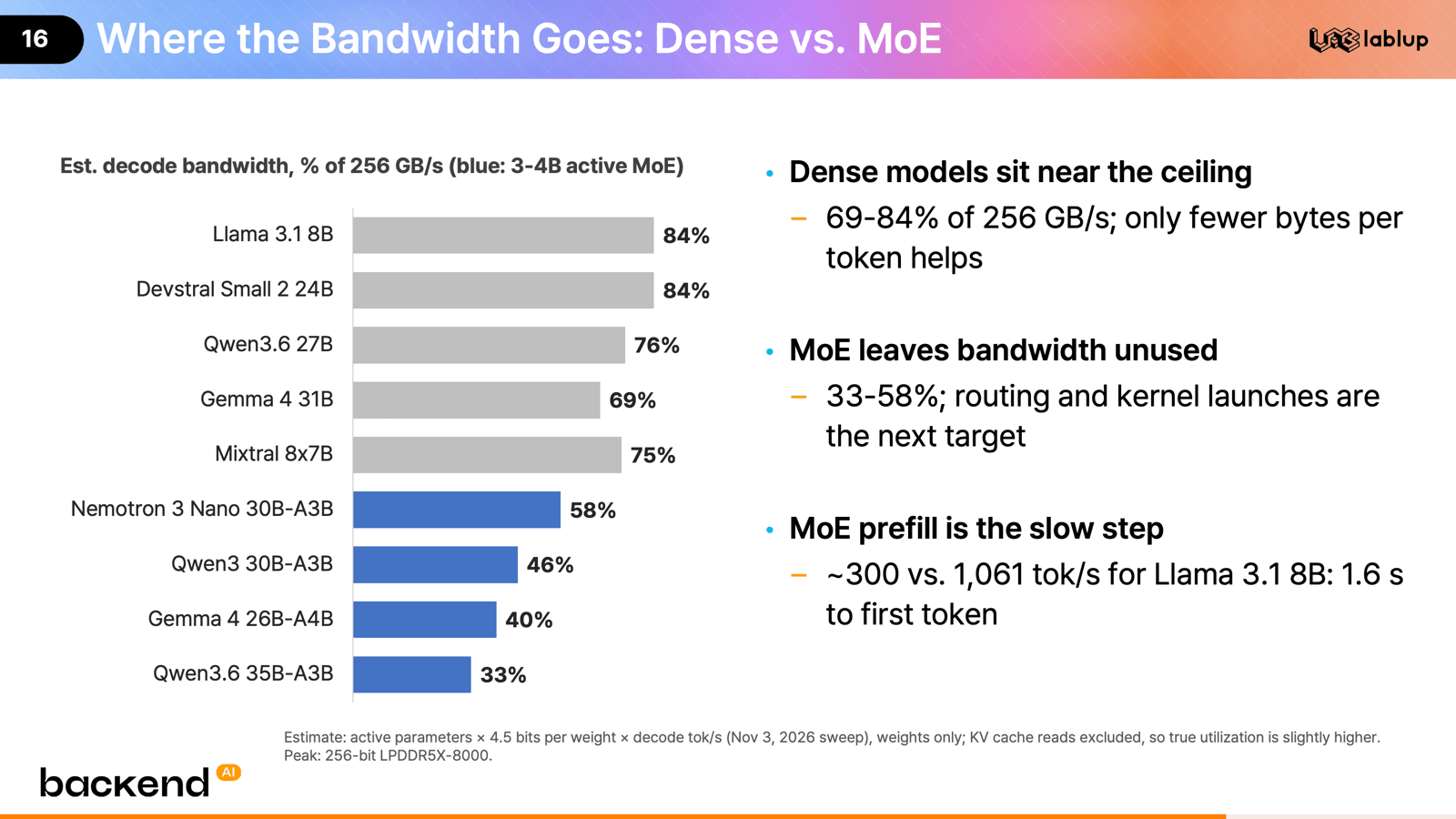
Dense models use 69–84% of the theoretical maximum. These figures exclude KV cache reads, so actual utilization is slightly higher. To go faster from here, we need to reduce the number of bytes read per token. MoE models with 3–4B active parameters, on the other hand, reach only 33–58%. That means there is bandwidth to spare, and the next optimization targets are expert routing and kernel launch overhead.
Prefill is where MoE models fall short. At about 300 tok/s, they trail far behind Llama 3.1 8B's 1,061 tok/s, and a 512-token prompt takes 1.6 seconds to produce the first token.
Batch serving
We ran mlxcel-server with --parallel 4 and compared sending 1 and 4 concurrent requests, each generating 128 tokens from a 512-token prompt. Concurrent runs started with a warm prompt cache, and aggregate throughput includes prefill.
| Model | Aggregate throughput 1 request | Aggregate throughput 4 requests | Scaling | Per-request cost |
|---|---|---|---|---|
| Llama 3.1 8B | 34 tok/s | 69 tok/s | 2.0× | Per-request decode 41 → 19 tok/s |
| Qwen3 30B-A3B | 37 tok/s | 68 tok/s | 1.9× | Time to first token 1.6 → 3.1 s |
With 4 concurrent requests, total throughput roughly doubles, but each individual request slows down. On a single-user PC, batch 1 is the better fit; in environments where multiple users or agents share the machine, batch serving makes more sense.
Wrapping up
Starting with 0.8, MLxcel supports Apple Silicon, NVIDIA, and AMD ROCm from a single MLX-based Rust engine, with no Python layer in the request path. On Strix Halo, all 44 models we tested ran successfully, a dense 31B model decodes at 10.2 tok/s, close to the memory bandwidth ceiling, and 30B-A3B MoE models decode at up to 76 tok/s.
Here are three things we learned from porting to Strix Halo:
- Budget memory against the device pool. On a design where the memory the OS sees differs from the memory the GPU uses, the engine has to change its assumptions, even under the same "unified memory" label.
- Profile before you port. GPU time, not call count, set the priorities, and we ended up porting kernels in nearly the opposite order from our original plan.
- MoE benefits most from unified memory. MoE models with few active parameters run several times faster than dense models of the same size, and they still have bandwidth to spare.
What's next
MoE is first on the list. MoE models with 3–4B active parameters still use only 33–58% of available bandwidth, so cutting expert routing and kernel launch overhead should push decode speed higher. We also plan to improve MoE prefill, which is currently stuck at around 300 tok/s.
Next is broader hardware support. The ROCm backend is still experimental and validated only on gfx1151. From here, we want to extend support to the CDNA architecture used in Instinct datacenter GPUs. CDNA 3 and CDNA 4 have wave64, MFMA, and hardware FP8 and FP4, so they need a separate kernel path. CDNA 5, on the other hand, has been redesigned on an RDNA foundation and uses wave32, so the kernels we wrote for Strix Halo can serve as a starting point.
Try it out
MLxcel is open source under the Apache 2.0 license. Grab the source from the GitHub repository and build with --features rocm to start using it on Strix Halo right away. The full list of changes is in the v0.8.0 and v0.8.1 release notes. Issues and pull requests are always welcome, and results from AMD GPUs other than gfx1151 would be especially helpful as we expand hardware support.
If you're interested in bringing MLxcel into your organization's AI infrastructure, contact Lablup at contact@lablup.com.
References
- lablup/mlxcel, mlxcel release notes
- AMD Ryzen AI Max+ 395 product page
- Tom's Hardware: Strix Halo unveiled
- TechPowerUp: Strix Halo chiplet layout
- ServeTheHome: GB10 SoC architecture (Hot Chips 2025)
- PC Gamer: GB10 and the MediaTek collaboration
- Chips and Cheese: Grace Hopper
- Chips and Cheese: CDNA 5 interview
- Electronic Design: Kaveri and hUMA
- Apple M1 announcement
- Tom's Hardware: NVIDIA RTX Spark
- Neowin: Copilot+ PC requirements
- Stream HPC: RDNA and CDNA similarities and differences
- ml-explore/mlx #2300: ROCm backend proposal
- IREE: ROCm deployment guide
